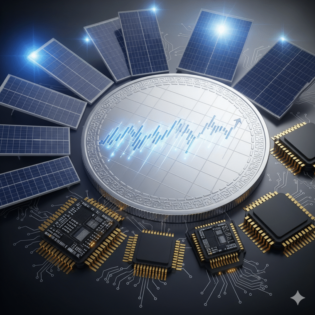

1. The Renaissance of Pure-Play Flash
The semiconductor industry is witnessing a structural transformation. The year 2025 marks the definitive return of SanDisk Corporation (NASDAQ: SNDK) as an independent market force.
This resurgence follows its strategic spin-off from Western Digital on February 21, 2025.¹ The separation has unlocked significant shareholder value. It has allowed SanDisk to shed the conglomerate discount that historically depressed its valuation. The market response has been unequivocal.
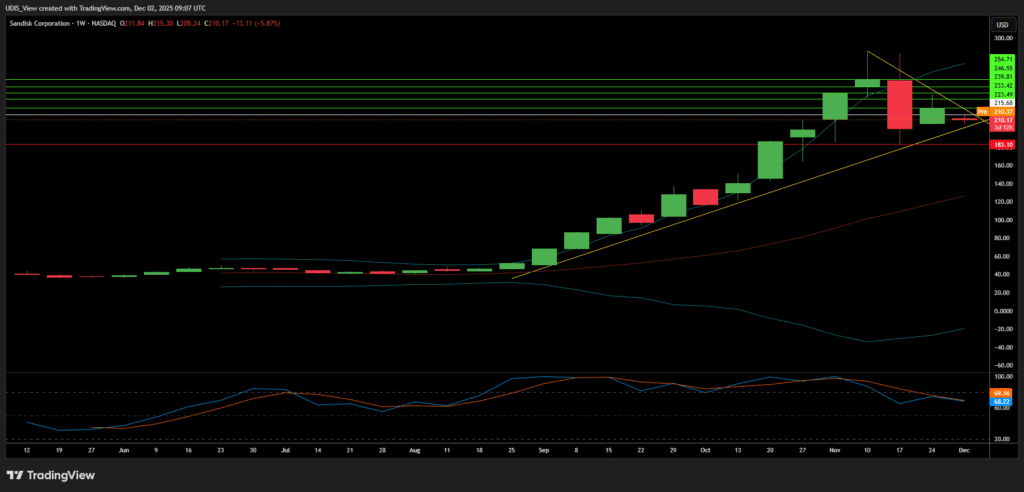
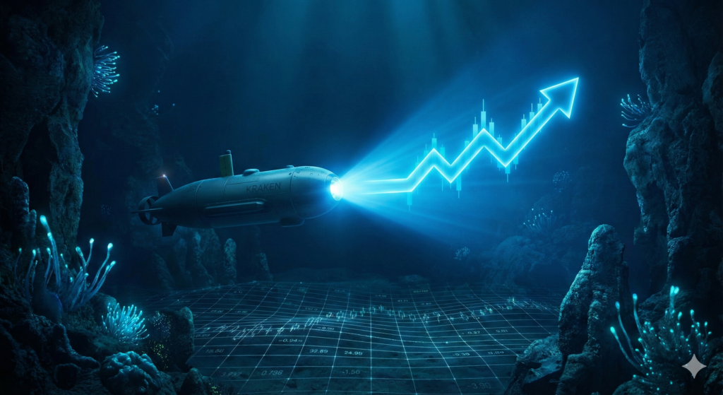
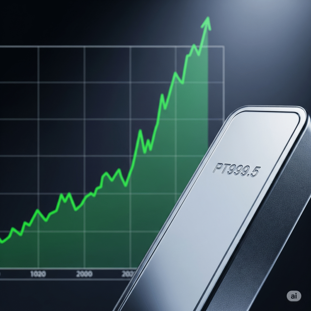
Stock prices have surged toward $230 per share by November 2025.² Major financial institutions now project targets as high as $273.³
This report analyzes the convergence of factors driving this ascent. We examine the geopolitical maneuvering behind SanDisk’s manufacturing pivot, analyze the physics of its new BiCS8 technology, and explore the macroeconomic currents creating a “storage supercycle.” SanDisk is no longer merely a component vendor; it has become a critical infrastructure provider for the Artificial Intelligence economy.
1.1 The Strategic Rationale of the Spin-Off
The separation of Western Digital’s Hard Disk Drive (HDD) and Flash businesses resolved a long-standing valuation disconnect. Investors long argued that the conglomerate structure obscured the high-growth potential of flash memory.
The spin-off distributed 80.1% of SanDisk shares to WDC stockholders.⁴ This distribution created a pure-play entity capable of navigating the volatile semiconductor cycle with agility. The split allowed SanDisk to adopt a capital allocation strategy tailored to flash memory dynamics.
Flash memory requires massive, cyclical capital expenditures (CapEx), whereas HDDs operate on a slower, cash-cow model. Separating these balance sheets prevents the capital needs of one from cannibalizing the other. SanDisk now operates with a sharpened strategic focus, pursuing disruptive memory technologies without the burden of legacy magnetic storage assets.
Spin-Off Execution Details:
| Metric | Detail | Source |
| Completion Date | February 21, 2025 | ¹ |
| Distribution Ratio | 80.1% to WDC Shareholders | ⁴ |
| Remaining Stake | WDC retains ~19.9% (gradual sell-down) | ¹ |
| Ticker Symbol | NASDAQ: SNDK | ⁵ |
| S&P 500 Inclusion | Replaced Interpublic Group | ⁶ |
1.2 The “Index Effect” and Market Validation
SanDisk’s reintegration into the S&P 500 index in late 2025 served as a massive technical catalyst.⁶ Index inclusion forces passive funds and ETFs to acquire shares, creating a floor of structural buying pressure unrelated to fundamental performance.
The “Index Effect” reduces cost of capital, increases stock liquidity, and signals stability to institutional investors. SanDisk’s market capitalization stabilized above $30 billion shortly after the spin-off.⁷ This valuation validates the market’s appetite for a standalone flash memory giant and distinguishes SanDisk from smaller, more volatile semiconductor competitors.
1.3 Executive Leadership and Vision
CEO David Goeckeler has steered the company through this transition. His strategy focuses on margin expansion and technological leadership. The management team has prioritized “friend-shoring” the supply chain and focused on product mix-shifts toward high-margin enterprise SSDs.
This leadership has been instrumental in navigating the post-separation landscape, successfully executing complex asset divestitures in China while ramping up advanced manufacturing in Japan.
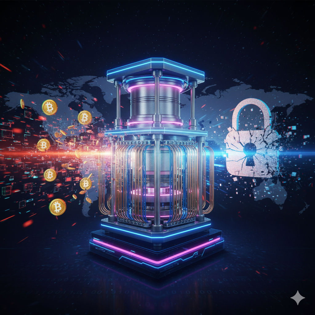
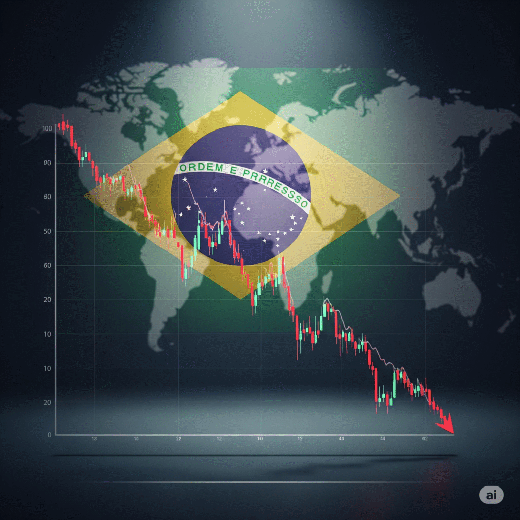
2. Macroeconomic Analysis: The 2025 Storage Supercycle
The global economy is entering a period of renewed hardware investment driven by the need to upgrade infrastructure for the AI era. This phenomenon, termed the “Storage Supercycle,” acts as a rising tide for SanDisk.
2.1 The Crystal Cycle: Boom, Bust, and Recovery
The memory market is notorious for its “Crystal Cycle” the violent oscillations between shortage and glut. The industry experienced a severe downturn in 2023 and 2024 as prices collapsed due to inventory bloat.
Manufacturers responded with unprecedented discipline. Major players like Samsung, SK Hynix, and Western Digital/SanDisk slashed production, cut utilization rates to historic lows, and deferred billions in capital expenditures. These decisions have created a structural supply deficit for 2025.
The Lag Effect:
Building new semiconductor cleanrooms takes 18 to 24 months.⁸ Equipment installation adds further delays. The capacity cuts made in 2023 mean that new supply cannot physically come online until late 2026. This creates a “supply air pocket” where demand is accelerating while supply remains constrained by physics and construction timelines.
2.2 The 2025 Supply-Demand Imbalance
The consequences of this under-investment are now visible. TrendForce reports a sharp tightening of wafer supply in November 2025.⁹ Contract prices for NAND flash wafers have surged by over 60% in some categories.¹⁰
This is a seller’s market. SanDisk now possesses significant pricing power. Negotiations with hyperscalers (Amazon AWS, Microsoft Azure, Google Cloud) have shifted; customers are no longer demanding quarterly price cuts. They are locking in long-term supply agreements (LTAs) to ensure continuity.¹¹ Prices are rising double-digits sequentially, directly expanding SanDisk’s gross margins.
2.3 Elasticity of Demand in the AI Era
Traditional economic theory suggests that higher prices reduce demand. However, demand for storage in the AI era is inelastic. AI model training cannot proceed without massive data lakes, and inference engines cannot function without high-speed retrieval systems.
Corporations racing to deploy Generative AI view storage as a strategic necessity. They absorb price increases to avoid project delays. This decoupling of demand from price sensitivity is a rare economic phenomenon fueling the “Supercycle.” SanDisk is uniquely positioned to capture this value as its product portfolio is heavily weighted toward the high-capacity enterprise drives required for these workloads.
2.4 Inflationary Pressures and Input Costs
The pricing environment is favorable, but inflation poses risks. The cost of raw materials has risen. Rare earth elements are critical for semiconductor manufacturing. China has imposed export restrictions on Gallium and Germanium.¹² This has increased input costs for wafers.
However, SanDisk’s transition to advanced nodes mitigates this. The BiCS8 technology increases bit density by 50%.¹³ This means SanDisk produces more gigabytes per wafer. The efficiency gain effectively lowers the cost per bit, offsetting the inflationary pressure on raw materials. This operational leverage is key to margin expansion in an inflationary environment.
Macroeconomic Indicators:
| Indicator | Trend | Impact on SanDisk |
| NAND Contract Price | +60% Surge (Nov 2025) | Direct Revenue/Margin Growth ⁹ |
| CapEx Spend (Industry) | Flat/Modest Growth | Sustained Supply Shortage ¹⁴ |
| AI Infrastructure Spend | >$1 Trillion by 2030 | Long-term Demand Tailwinds ¹⁵ |
| Interest Rates | Stabilizing | Lower Cost of Debt for CapEx |
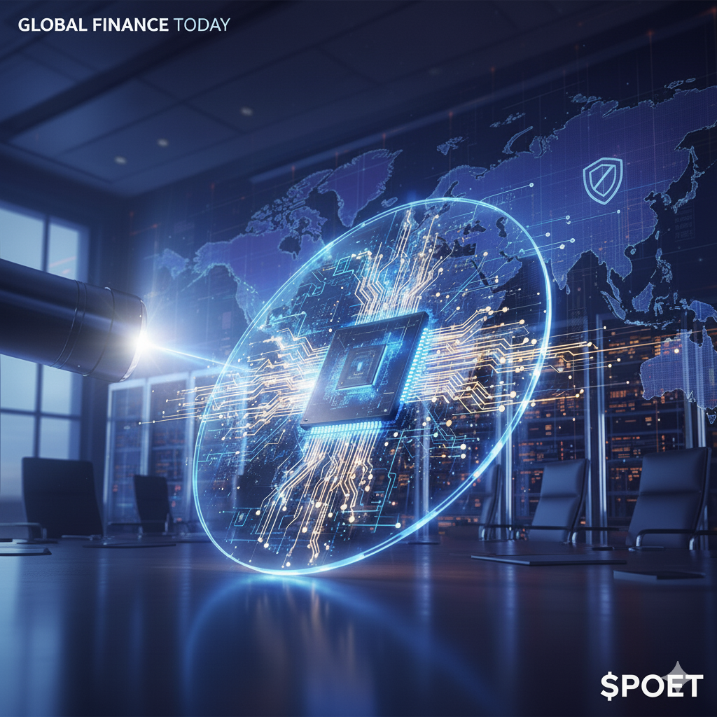
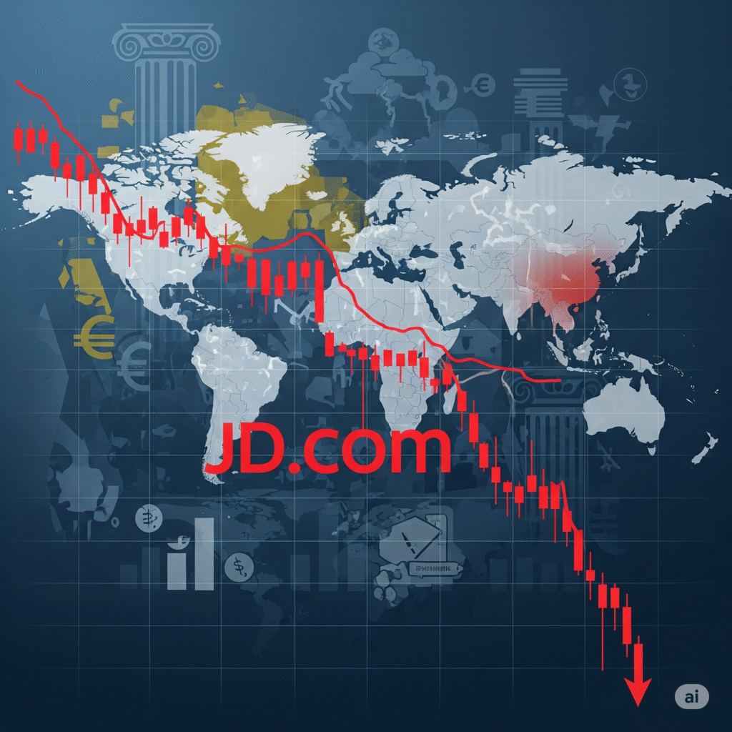
3. Geostrategy: Navigating the Chip War
SanDisk operates at the fault line of the US-China semiconductor conflict. Its strategy in 2025 is defined by aggressive de-risking and realigning its supply chain to match the new geopolitical reality.
3.1 The JCET Transaction: Strategic Asset Lightness
In a masterful geopolitical maneuver, SanDisk divested its Shanghai manufacturing assets. It sold an 80% equity interest in SanDisk Semiconductor (Shanghai) Co. Ltd. (SDSS). The buyer was JCET Management Co., Ltd., a Chinese technology conglomerate.¹⁶ The deal was valued at approximately $624 million.¹⁷
Strategic Implications:
- Regulatory Insulation: Majority ownership transferred to a Chinese entity, making the facility less vulnerable to Beijing’s retaliatory measures against US firms.
- Capital Efficiency: SanDisk reduced its fixed capital expenditures, shifting to a variable cost model for assembly and testing in China.¹⁶
- Market Access: The joint venture structure preserves access to the Chinese domestic market and complies with “Made in China” localization preferences.
SanDisk retains a 20% stake,¹⁷ ensuring continued influence without bearing the full geopolitical risk. The transaction decoupled SanDisk’s manufacturing assets from its intellectual property, which remains firmly under US control.
3.2 US Export Controls and the Entity List
The US Department of Commerce has expanded export controls. New rules restrict the export of equipment for producing NAND with 128 layers or more to China.¹⁸ These rules aim to freeze China’s semiconductor development.
SanDisk is insulated from these restrictions as its primary wafer fabrication occurs in Japan, not China. The company partners with Kioxia (formerly Toshiba Memory) with fabs located in Yokkaichi and Kitakami.¹⁹ This Japanese manufacturing base is a critical geostrategic asset, placing SanDisk inside the “Chip 4” alliance (US, Japan, Taiwan, Korea).
Alliance Benefits:
- Access to Tools: SanDisk fabs have unrestricted access to advanced lithography tools from ASML (Netherlands) and Applied Materials (US), unlike Chinese competitors like YMTC.
- Material Supply: Japan dominates the supply of photoresists and etching gases, ensuring SanDisk priority access to these critical consumables.
3.3 The Rise of Malaysia: The “China Plus One” Pivot
SanDisk is actively diversifying its backend operations. As it reduces reliance on China, it expands in Malaysia, which has emerged as the global hub for chip packaging and testing, now controlling 13% of the global market.²⁰
Why Malaysia?
- Geopolitical Neutrality: Malaysia maintains balanced relations with both the US and China, acting as a “safe harbor.”
- Ecosystem Maturity: The Penang region hosts a dense cluster of suppliers including Intel, Micron, and ASE.²¹
- TAA Compliance: Western hyperscale customers (Microsoft, AWS) require Trade Agreements Act (TAA) compliance. Products manufactured in Malaysia meet these requirements, whereas products from China often do not.¹⁷
This shift mitigates the risk of supply chain paralysis from tensions over Taiwan or the South China Sea.
3.4 The Japan Alliance: Kioxia Joint Venture
The partnership with Kioxia is the cornerstone of SanDisk’s manufacturing strategy. The joint venture operates the world’s largest flash memory fabs. In 2025, they inaugurated “Fab2” in Kitakami.¹⁹
Fab2 Capabilities:
- AI-Driven Production: The facility uses AI to optimize yield and production flow.¹⁹
- Earthquake Resilience: Advanced seismic isolation structures protect billion-dollar equipment.
- Government Subsidies: The Japanese government subsidizes a portion of the investment,¹⁹ reducing SanDisk’s capital burden.
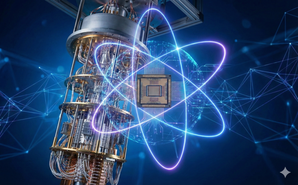
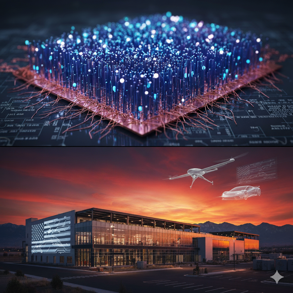
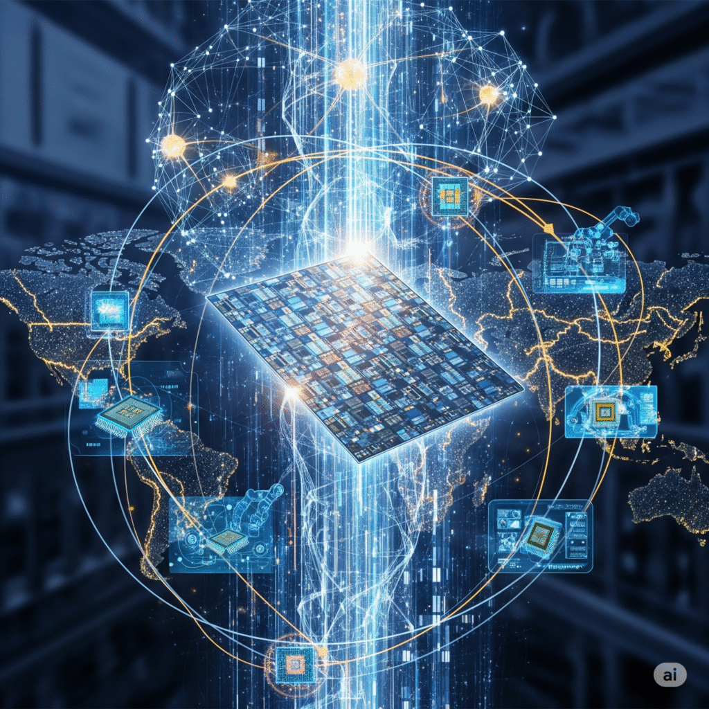
4. Technology and Physics: The BiCS8 Revolution
SanDisk’s valuation premium is underpinned by its technology. The company has moved beyond simple 3D stacking, leveraging advanced material science and hybrid bonding physics.
4.1 3D NAND Scaling Limits
Traditional 3D NAND scaling is hitting physical walls. Etching a channel hole through 200+ layers of silicon is difficult; the hole tends to taper or twist, destroying memory cells at the bottom. Furthermore, memory cells require high-temperature processing for reliability, while the control logic (CMOS) degrades at those temperatures. Building both on the same wafer forces a compromise.
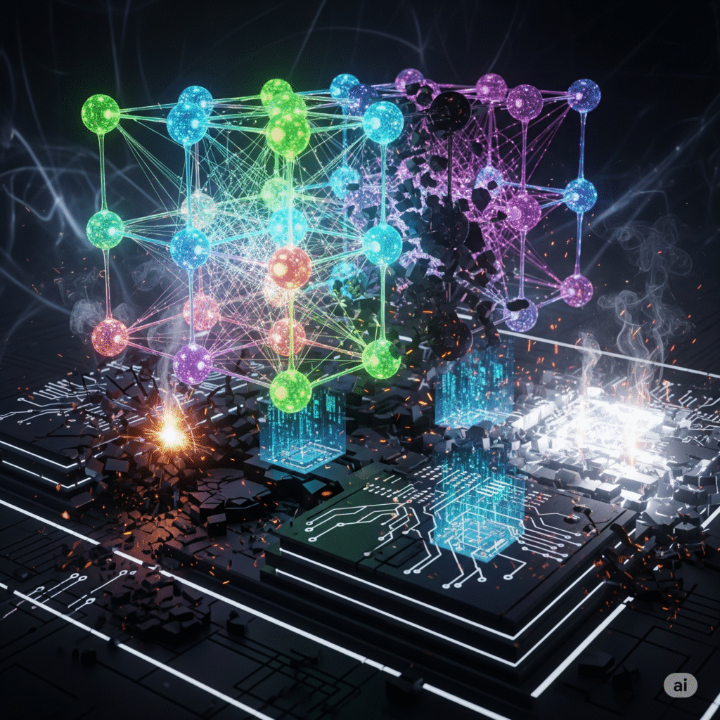
4.2 CMOS Bonded to Array (CBA) Architecture
SanDisk’s BiCS8 (8th Generation Bit Cost Scalable) technology solves this physics problem using CMOS Bonded to Array (CBA) architecture.¹³
The CBA Process:
- Wafer 1 (The Array): Memory cells are fabricated on one wafer at high temperatures to maximize reliability.
- Wafer 2 (The Logic): Control logic is fabricated on a separate wafer, allowing the use of advanced, high-speed CMOS nodes (14nm or smaller).
- Hybrid Bonding: The two wafers are flipped and bonded face-to-face with copper interconnects joining them with atomic precision.
Technical Advantages:
- I/O Speed: The logic wafer drives data faster. BiCS8 achieves I/O speeds of 3.2Gb/s to 4.8Gb/s.²³
- Bit Density: The memory array uses 218 layers.¹³ Because logic is moved to a separate wafer, array density increases by 50% compared to BiCS5.¹³
- Yield: Defects in the logic do not ruin the memory array.
4.3 High Bandwidth Flash (HBF): Solving the Memory Wall
A critical bottleneck in AI computing is the “Memory Wall.” SanDisk is pioneering High Bandwidth Flash (HBF).²⁴
Concept: Replace or augment HBM with 3D NAND connected via high-speed logic interposers. An 8-high HBF stack offers 3.12 Petabytes (PB) of capacity,²⁴ whereas HBM stacks offer only Gigabytes. This is critical for AI Inference, where massive LLMs require holding terabytes of parameters in memory.
SanDisk has formed a technical advisory board with SK Hynix to standardize this technology,²⁵ positioning itself as a leader in the “AI Edge” market.
4.4 UltraQLC: The Physics of Quad-Level Cells
SanDisk has pushed the boundaries of Quad-Level Cell (QLC) reliability. QLC stores 4 bits per cell, requiring the distinction between 16 distinct voltage levels. To solve the challenge of razor-thin voltage margins, SanDisk’s UltraQLC platform uses advanced error correction algorithms.²⁶
This innovation enables enterprise SSDs with capacities up to 122.88TB,²⁶ allowing QLC drives to replace Hard Disk Drives (HDDs) in “warm” storage tiers.
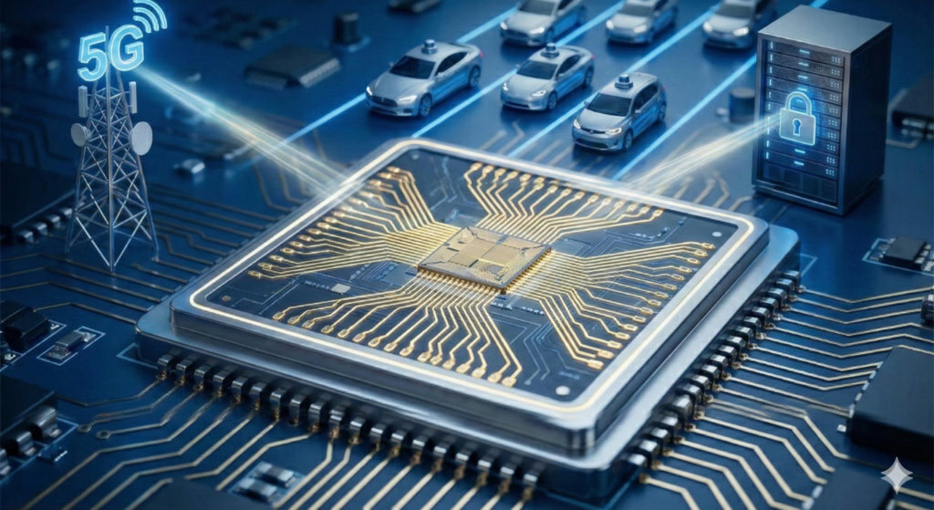
5. AI and Data Center Architecture
SanDisk’s product strategy aligns with the architectural shift in data centers from CPU-centric to Data-centric computing.
5.1 The Data Lake Explosion
AI models require training data sets measured in exabytes. SanDisk’s 122TB UltraQLC SSD (SN670) is designed for these high-performance repositories.²⁶ It offers the density of HDDs with the speed of flash, allowing data centers to consolidate racks of HDDs into a single shelf of QLC SSDs, reducing floor space and cooling power.
5.2 Enterprise SSDs: The Growth Engine
The SanDisk DC SN861 is the flagship PCIe Gen5 NVMe SSD.²⁷
- Performance: Read speeds reach 13,700 MB/s. Random read IOPS hit 3.3 million.²⁷
- Standards: Compliant with OCP 2.0 (Open Compute Project),²⁸ ensuring compatibility with hyperscale server designs.
Product Specification Comparison:
| Feature | DC SN861 (Performance) | DC SN670 (Capacity) |
| Capacity Max | 15.36 TB | 122.88 TB |
| NAND Type | TLC (Triple Level Cell) | UltraQLC (Quad Level Cell) |
| Interface | PCIe Gen5 | PCIe Gen5 |
| Use Case | AI Training / Compute | Data Lakes / AI Ingest |
| Endurance | 1-3 DWPD | 0.35 DWPD |
| Source | ²⁷ | ²⁶ |
5.3 Power Efficiency and ESG
Power is the limiting factor for AI data centers. The SN861 leads the industry in IOPS per Watt.²⁷ SanDisk reports focus on reducing the carbon footprint of the manufacturing process,²⁹ with the shift to BiCS8 reducing the energy required to manufacture each gigabyte of storage.
6. Financial Analysis: Valuation and Performance
6.1 Fiscal Q4 2025 Performance
SanDisk reported strong results for the fiscal fourth quarter of 2025:
- Revenue: $1.901 billion, representing an 8% year-over-year increase.³⁰
- Gross Margin: Non-GAAP gross margin expanded to 26.4%, a 3.7 percentage point increase quarter-over-quarter.³⁰
- Cloud: Revenue grew 25% year-over-year to $213 million,³⁰ confirming hyperscalers have resumed spending.
- Consumer: Revenue rose 12% to $585 million.³⁰
6.2 The Bull Case Valuation
Analysts at Morgan Stanley have rated SanDisk “Overweight,” raising the price target to $273 in November 2025.² The valuation is driven by EPS growth potential as pricing power returns.
6.3 Liquidity and Capital Allocation
SanDisk achieved a net cash position of $91 million months ahead of schedule.³¹ This proves the company can generate cash even while investing in capacity.
7. Legal, Cyber, and Patent Analysis
7.1 The Polaris PowerLED Victory
SanDisk was sued by Polaris PowerLED Technologies, LLC for alleged patent infringement.³² In July 2025, the Patent Trial and Appeal Board (PTAB) denied institution of Polaris’s IPRs,³² a major defensive victory that neutralizes the threat of costly injunctions.
7.2 Pre-Spin Indemnification
Before the spin-off, Western Digital faced a $500 million judgment regarding SPEX Technologies’ patents.³³ The separation agreement clarifies liability, protecting SanDisk’s standalone balance sheet.
7.3 Cybersecurity Standards
- TCG Opal 2.01: Drives support Self-Encrypting Drive (SED) standards.²⁶
- FIPS 140-3: SanDisk pursues validation for US government agencies.³⁴
- Supply Chain Security: SanDisk contributes to the OCP S.A.F.E. initiative,³⁵ ensuring firmware integrity.
8. Risks and Challenges
- China Market Volatility: Any expansion of China’s “Unreliable Entity List” could impact sales.¹²
- Technological Execution Risk: Yield issues at the Kitakami Fab2 could constrain supply of BiCS8 wafers.
- The Cyclical Trap: If the industry over-invests in 2026, a glut could emerge by 2028.
9. Conclusion: The Strategic Pivot
SanDisk’s performance in 2025 serves as a masterclass in corporate strategy. The spin-off was timely, liberating the company to pursue a pure-play flash strategy aligned with the AI boom.
Investment Verdict:
The analysis supports the “Overweight” rating assigned by major analysts. The structural tailwinds of the AI Supercycle, combined with SanDisk’s operational discipline, present a compelling case for value creation.
Addendum: Detailed Data Tables
Table A: Analyst Price Targets (November 2025)
| Firm | New Target | Previous Target | Rating | Date | Source |
| Morgan Stanley | $273 | $263 | Overweight | Nov 24, 2025 | ² |
| Jefferies | $180 | $60 | Buy | Q4 2025 | ³⁶ |
| Benchmark | $125 | $85 | Buy | Q4 2025 | ³⁶ |
| Mizuho | $112 | $57 | Buy | Q4 2025 | ³⁶ |
Table B: Product Roadmap & Technology
| Technology Node | Layers | Architecture | Key Feature | Status | Source |
| BiCS5 | 112 | CUA | Legacy Volume | Phasing Out | ¹³ |
| BiCS6 | 162 | CUA | Transitional | Production | ¹³ |
| BiCS8 | 218 | CBA (Bonded) | 50% Density Boost | Ramping | ¹³ |
| BiCS Next | >300 | CBA + String Stacking | 1Tb TLC Die | In Development | ²⁴ |
Table C: Key Manufacturing Locations
| Facility | Location | Role | Partner/Owner | Strategic Value | Source |
| Yokkaichi Plant | Mie, Japan | Wafer Fab | Kioxia JV | Mature Hub | ¹⁹ |
| Kitakami Fab2 | Iwate, Japan | Wafer Fab (BiCS8) | Kioxia JV | Advanced Node | ¹⁹ |
| SDSS | Shanghai, China | Assembly/Test | JCET (80%) / SNDK (20%) | China Market Access | ¹⁶ |
| Penang | Malaysia | Assembly/Test | Contract Partners | TAA Compliance | ²¹ |
SanDisk Long (Buy)
Enter At: 215.68
T.P_1: 223.49
T.P_2: 233.42
T.P_3: 239.81
T.P_4: 246.55
T.P_5: 254.71
S.L: 183.10