
Samsung Electronics stands at a critical juncture in the global technology landscape. While a dominant force in memory chips, its semiconductor foundry business has faced significant challenges. Recent strategic maneuvers, particularly a landmark deal with Tesla, signal a potential turning point. This analysis examines the multifaceted factors that have driven Samsung’s trajectory, encompassing geopolitical shifts, macroeconomic forces, technological advancements, and intellectual property strategies.
The Tesla Catalyst: A Strategic Inflection Point
A pivotal development for Samsung’s foundry operations is its substantial contract with Tesla. This agreement provides a crucial anchor client, potentially revitalizing a segment facing considerable pressure.
The $16.5 Billion Deal: Details and Confirmation
Samsung Electronics secured a 22.8 trillion-won ($16.5 billion) contract to supply semiconductors.1 This agreement became effective on July 26, 2024, and extends until December 31, 2033.1 Tesla CEO Elon Musk later confirmed Samsung as the counterparty on X.1 He stated Samsung’s new Texas fabrication facility “will be dedicated” to producing Tesla’s next-generation AI6 chip.1
Musk underscored the “strategic importance” of this arrangement.1 He also noted Tesla’s role in maximizing manufacturing efficiency.1 Musk even hinted that the deal’s value might exceed the announced $16.5 billion.1
This dedication to Tesla provides a guaranteed revenue stream for the Texas fab.6 The facility previously faced delays and struggled to secure major customers. 4 Tesla’s public commitment, amplified by Musk’s involvement, validates Samsung’s substantial U.S. investment.6 This transforms the fab from a potential liability into a strategic asset. Such a high-profile partnership could attract additional U.S. clients. This leverages CHIPS Act incentives and strengthens American firms’ supply chain resilience.
Revitalizing the Foundry Business: A New Anchor Client
Samsung’s foundry business has incurred significant losses. These losses were estimated to exceed 5 trillion won ($3.63 billion) in the first half of 2025.4. Analysts, including Pak Yuak from Kiwoom Securities, anticipate this deal will help mitigate these financial setbacks.4 The contract represents a major victory for Samsung’s contract manufacturing services. This division currently trails Taiwan Semiconductor Manufacturing Company (TSMC).2 Projections suggest this deal could boost Samsung’s foundry revenue by 10% annually.3
The foundry division’s profitability has been impacted by lower utilization rates.9 High research and development (R&D) expenses for advanced nodes also contributed to these challenges.9 Securing a long-term, high-value contract directly addresses the utilization issue. It provides a stable revenue base. This financial stabilization is crucial for reinvesting in advanced technology. It also helps in regaining investor confidence. A more stable foundry business allows Samsung to be more aggressive in its R&D. It also strengthens its competitive stance against TSMC, particularly for next-generation nodes.
Tesla’s Strategic Imperative: Supply Chain Resilience and AI Advancement
Tesla’s decision to diversify its chip sourcing beyond TSMC enhances its supply chain resilience.1 TSMC will produce Tesla’s AI5 chip.1 The AI6 chip, to be manufactured by Samsung, is vital for Tesla’s Full Self-Driving (FSD) v13 platform.5 It is also critical for broader AI computing initiatives.5
Musk’s statement about Tesla assisting in maximizing manufacturing efficiency points to a deeper collaboration.1 His personal involvement, stating he will “walk the line personally,” suggests active participation in production optimization.1 This indicates Tesla is not merely purchasing chips. It is actively contributing to the manufacturing process, possibly sharing design-for-manufacturability insights. This represents a form of vertical integration for Tesla and co-innovation for Samsung. This collaborative model, if successful, could become a new trend in high-tech manufacturing. Major clients might directly engage with foundries to accelerate production and optimize yields for highly specialized chips. It also highlights the growing importance of AI-specific hardware, driving demand for advanced foundry services.
Samsung-Tesla Chip Deal: Key Contractual Terms
| Term | Detail |
| Contract Value | $16.5 Billion (22.8 Trillion Won) |
Navigating the Semiconductor Foundry Landscape
Samsung operates in a highly competitive semiconductor foundry market. Its position is defined by market share dynamics, ongoing yield rate challenges, and the intense race for high-bandwidth memory (HBM) leadership.
Market Share Dynamics: The Widening Gap with TSMC
TSMC consistently dominates the global foundry market. In Q4 2024, TSMC’s market share reached 67.1%.10 Samsung’s share, in contrast, declined to 8.1% from 9.1% in Q3 2024.10. This widened the market share gap to 59 percentage points.10 Earlier, in Q3 2024, TSMC held 64.9%, while Samsung held 9.3%.11 Samsung’s share further decreased to 7.7% in Q1 2025.8
TSMC’s growth stems from robust demand for AI servers and flagship smartphone application processors (APs).10 New PC platforms also contribute significantly.10 Samsung’s revenue declined as gains from new advanced semiconductor clients did not fully offset reduced orders from key existing customers.10 Samsung’s market share decline, despite its technological capabilities, highlights a critical customer acquisition challenge.10 Analysts explicitly state Samsung needs to secure “big clients” beyond its internal needs to reduce losses and compete effectively.12 The Tesla deal represents a significant step in this direction. It offers a potential blueprint for attracting other major players. Samsung’s future in the foundry market depends on its ability to convert technological advancements into strong client relationships. This is particularly true for high-volume, high-margin orders, which currently favor TSMC.
Global Foundry Market Share: Samsung vs. TSMC (2019-2025)
| Quarter/Year | TSMC Market Share (%) | Samsung Market Share (%) | Gap (TSMC – Samsung) (%) |
| Q1 2019 | 48.1 | 19.1 | 29.0 |
| Q3 2024 | 64.9 | 9.3 | 55.6 |
| Q4 2024 | 67.1 | 8.1 | 59.0 |
| Q1 2025 | 67.6 | 7.7 | 59.9 |
Yield Rate Challenges: The Path to 2nm Supremacy
Samsung’s foundry business has consistently struggled with yield rates.13 Manufacturing consistency, especially with its 3nm process launched in 2022, also presented difficulties.13 For its 2nm trials, Samsung’s yield was approximately 30% at the start of 2025.14 The company aims for 50% and requires 70% for viable mass production of chips like the Exynos 2600.14 Some reports indicate yields approaching 40%.16
TSMC’s 2nm process began risk production in late 2024.13 Mass production is targeted for 2025, with reported yields up to 70%.13 Samsung was the first to adopt Gate-All-Around (GAA) technology for its 3nm node.18 TSMC will apply GAA to its 2nm process 15
While nanometer size indicates technological leadership, the yield rate is the critical factor for profitable mass production.14 Samsung’s early adoption of GAA for 3nm did not translate into market dominance due to yield issues.13 The Tesla deal, while significant, is unlikely to utilize Samsung’s cutting-edge 2nm node due to these constraints.5 This indicates that proving a 2nm yield remains a major hurdle for Samsung. It needs to attract more top-tier clients like Nvidia and Qualcomm for their most advanced chips.12 Samsung’s innovation strategy must prioritize yield stabilization and improvement alongside node shrinkage. Success with the Tesla AI6 chip, even if on a more mature node, could build confidence for future advanced node orders. The focus should be on reliable advanced manufacturing, not just early advanced manufacturing.
High-Bandwidth Memory (HBM): Competing in the AI Era
Samsung has fallen behind SK Hynix and Micron in high-bandwidth memory (HBM) chips.1 These are crucial components for AI chipsets.1 SK Hynix leads HBM shipments and is the primary supplier to Nvidia.20 It has achieved record profits driven by HBM demand.20
Samsung struggled to pass Nvidia’s HBM3E qualification tests.1 This pushed its plans to at least September 2025, despite redesigning its chip.1 Samsung recently delivered HBM3E 12-layer chips for AMD’s MI350X AI accelerators.19 This helped ease market doubts about its product quality.19 Samsung is also developing HBM4, aiming for 1c DRAM technology.19
The AI revolution is driving unprecedented demand for HBM.20 Samsung’s lag in HBM, particularly in securing Nvidia certification, directly impacts its ability to capitalize on the booming AI semiconductor market.20 The AMD deal is positive, but Nvidia’s certification is paramount for market leadership. This is due to Nvidia’s dominance in AI Graphics Processing Units (GPUs).19 Regaining HBM leadership is not just about memory market share. It is a strategic imperative for Samsung. It needs to position itself as a comprehensive AI semiconductor solutions provider, integrating memory and foundry capabilities. Failure to secure Nvidia’s HBM orders could further entrench SK Hynix’s lead. This would impact Samsung’s overall AI strategy.
Geopolitical Currents and Global Strategy
The semiconductor industry is deeply intertwined with global geopolitics. Samsung’s strategic decisions reflect this complex interplay of trade, tariffs, and international alliances.
US-South Korea Alliance: Trade, Tariffs, and Tech Collaboration
South Korea’s semiconductor industry, valued at $548 billion, is a critical partner for the U.S. in achieving supply chain resilience.23 The U.S. is advocating for deeper collaboration in next-generation technologies. These include HBM4 and Extreme Ultraviolet (EUV) lithography.23 South Korea, in turn, seeks tariff relief to protect its 60% global DRAM market share.23 This is amidst threats of 25% U.S. tariffs on $140 billion in Korean exports.4
The Samsung-Tesla deal holds significant implications for South Korea. It aligns with the nation’s pursuit of deeper tech and trade ties with the U.S..4 The trade negotiations between the U.S. and South Korea are intricately linked to the semiconductor industry.23 The U.S. leverages its market access and CHIPS Act incentives. This encourages South Korean firms to onshore production or deepen collaboration. South Korea uses its dominant position in memory chips to seek tariff relief. The Samsung-Tesla deal, by bringing advanced chip manufacturing to the U.S., demonstrates South Korea’s commitment to this alliance. This could influence ongoing trade talks. This dynamic illustrates how national security and economic policy are increasingly intertwined with the global semiconductor supply chain. Samsung’s strategic investments are not purely commercial; they are also geopolitical chess moves aimed at securing favorable trade conditions and market access.
The CHIPS Act and Samsung’s US Investments: Building Resilience
Samsung’s Taylor, Texas fab represents its largest-ever U.S. investment.6 It initially totals $17 billion, with plans for over $37 billion in the region.6 The U.S. Department of Commerce awarded Samsung up to $4.745 billion in direct funding under the CHIPS and Science Act.6 This investment aims to strengthen the resilience of the U.S. semiconductor supply chain.6 It also seeks to advance U.S. technology leadership.6
The CHIPS Act funding and Samsung’s massive investment in Texas directly respond to global supply chain vulnerabilities.6 They also address geopolitical tensions, particularly with China.24 By building a comprehensive ecosystem in the U.S., Samsung and the U.S. aim to reduce reliance on potentially unstable regions. They also seek to create redundancy. The Tesla deal further solidifies this strategy. It provides a critical domestic customer for the U.S. fab. This trend of “friend-shoring” or regionalization of semiconductor manufacturing will likely continue. It is driven by government incentives and national security concerns. This could lead to a more diversified, but potentially more costly, global semiconductor production network. This would impact pricing and availability across various industries.
Strategic Diversification in a Fractured Supply Chain
South Korean firms are already relocating some manufacturing to Vietnam and Mexico.23 This mitigates potential tariff threats.23 Domestically, South Korea’s K-CHIPS Act offers tax incentives and R&D subsidies.22 The goal is to produce 30% of the world’s advanced chips by 2030.22
Samsung is not solely focusing on U.S. expansion. It is also investing heavily in its domestic “semiconductor mega-cluster” near Seoul.22 This dual strategy involves localizing advanced manufacturing capabilities within South Korea. It also includes expanding strategically in key markets like the U.S. This reflects a pragmatic approach to navigating a fractured global supply chain. It aims to secure both domestic technological leadership and international market access and resilience. This approach suggests that future semiconductor supply chains will be less about single points of failure. They will be more about distributed, strategically located hubs. This is driven by a complex interplay of economic incentives, national security, and technological advantage.
Innovation, Science, and Patent Power
Samsung’s long-term competitive edge is built upon its relentless commitment to R&D, its strategic patent portfolio, and its aggressive pursuit of next-generation manufacturing technologies.
Samsung’s R&D Commitment: Pushing Technological Frontiers
Samsung invests billions in R&D annually.25 This commitment is evident in its extensive patent portfolio.25 The company focuses on advanced manufacturing techniques. These include smaller process nodes like 5nm, 3nm, and 2nm.25 It also develops new materials.25 Samsung’s “semiconductor mega-cluster” near Seoul comprises five state-of-the-art chip plants.22 These focus on next-generation memory, such as 3D DRAM and V-NAND, and advanced foundry capabilities.22 The company has a $20 trillion investment in R&D infrastructure.22 This includes High NA EUV lithography and wafer bonding technology.22
Despite current yield challenges and market share struggles, Samsung’s consistent and massive R&D investment is a fundamental driver of its long-term competitiveness.9 This sustained commitment to pushing technological boundaries, from advanced nodes to new memory types, positions Samsung to potentially regain leadership in the future. The initial ramp-up costs and R&D expenses for advanced nodes have impacted recent profits.9 However, these are strategic investments for future growth. For a technology company like Samsung, R&D is not merely an expense. It is a strategic asset that ensures its relevance and leadership in rapidly evolving markets. This long-term view is crucial for investors assessing Samsung’s future value beyond short-term fluctuations.
The Strategic Value of Samsung’s Patent Portfolio
Samsung’s patents are strategic assets.25 They cover a wide range of semiconductor technologies, from design to manufacturing processes.25 Patents provide a competitive advantage. They protect technological advancements. They also offer strategic leverage in negotiations, such as licensing agreements and cross-licensing deals.25 Samsung utilizes patents to influence and shape industry standards. This ensures its technologies form the foundation for others.27
Samsung’s patent strategy extends beyond mere protection. It is a proactive tool for shaping industry standards and generating revenue through licensing.27 This allows Samsung to benefit even if competitors adopt technologies based on its patented innovations. The ability to cross-license also facilitates collaborative innovation. It reduces litigation risks, which is crucial in the highly litigious semiconductor industry. A strong and strategically managed patent portfolio provides a durable competitive advantage. This allows Samsung to monetize its R&D investments in multiple ways. It also helps maintain influence over the technological direction of the industry. This is a critical, often underestimated, aspect of its economic strength.
Advancements in 2nm Gate-All-Around (GAA) Technology
Samsung was the first to mass-produce the 3nm GAA process in 2022.18. However, it initially struggled with yield rates.18 The company is now working to improve yields for its upcoming 2nm process. 18 Mass production is targeted for the second half of 2025.14 Rumors suggest Qualcomm could place a 2nm chip order with Samsung if yields improve.12 Samsung’s 2nm Exynos 2600 chip is already in prototype mass production.14
Samsung’s early adoption of GAA for 3nm, despite initial yield issues, demonstrates its aggressive pursuit of next-generation transistor architecture.18 While challenging, mastering GAA at 2nm could give Samsung a performance and power efficiency edge over traditional FinFET designs. This could potentially attract high-value clients like Nvidia and Qualcomm for their cutting-edge chips.12 The rumored Qualcomm 2nm interest, though unconfirmed, highlights this potential.16 Success in 2nm GAA is crucial for Samsung to narrow the technology gap with TSMC. It is also vital for securing its position at the forefront of advanced chip manufacturing. This represents a significant technological gamble with high potential rewards if yield challenges are overcome.
Cybersecurity in the High-Tech Ecosystem
In the advanced semiconductor manufacturing sector, cybersecurity is not merely a technical concern but a fundamental strategic imperative. Protecting intellectual property and operational continuity is paramount.
Protecting Critical Infrastructure: Industry-Wide Imperatives
The semiconductor industry faces substantial cybersecurity threats.30 Incidents like TSMC’s 2018 WannaCry attack caused significant losses, totaling $84 million.30 The industry has since enhanced cybersecurity through a three-stage approach. This includes securing operational environments, inspecting inbound devices, and reinforcing supply chain cybersecurity.30 Collective action and collaboration are crucial. Organizations like SEMI and committees such as the Taiwan Semiconductor Cybersecurity Committee lead these efforts.30
As semiconductor manufacturing becomes more complex and interconnected, cybersecurity risks escalate.30 These threats endanger not only financial stability but also supply chain continuity and national security.30 The high value of individual wafers, potentially upwards of $20,000, means even minor disruptions can be catastrophic.30 Therefore, robust cybersecurity is not merely a compliance issue. It is a fundamental operational and strategic imperative for any major foundry. Companies like Samsung must continuously invest in advanced cybersecurity measures. They must also participate in industry-wide efforts. This protects their intellectual property, manufacturing processes, and customer data. This is a prerequisite for maintaining trust and securing critical contracts, especially in the defense and AI sectors.
Samsung’s Robust Security Protocols and Certifications
Samsung acknowledges the critical importance of securing its semiconductor technologies.31 These are designated as South Korea’s National Key Technologies.31 The company strengthens security measures through annual audits.31 It implements information security management systems, holding ISO 27001 and Common Criteria certifications.31 A dedicated Integrated Information Security Center also operates.31
Samsung enforces strict security management guidelines. It designates executive-level managers for technical security oversight.31 Non-Disclosure Agreements (NDAs) are concluded with corporate customers.31 Samsung’s detailed security protocols, government designations, and third-party certifications demonstrate a proactive and comprehensive approach to cybersecurity. This level of security is increasingly important for attracting and retaining high-profile clients. This is especially true for those in sensitive sectors like defense, automotive (Tesla), and AI. In these areas, intellectual property protection and supply chain integrity are paramount. In an era of escalating cyber threats, a strong cybersecurity posture becomes a competitive advantage. It builds trust with clients and mitigates risks that could otherwise derail major contracts and investments.
Conclusion: Charting Samsung’s Future Growth Trajectory
Samsung Electronics is navigating a complex and dynamic global landscape. Its future growth hinges on a strategic interplay of technological prowess, market adaptation, and geopolitical alignment.
Synthesizing Multi-Layered Drivers for Growth
The Tesla deal represents a significant economic and strategic victory for Samsung. It provides a crucial anchor client for its Texas fab. It also injects much-needed revenue into its foundry business. Samsung’s long-term growth depends on its ability to overcome yield challenges in advanced nodes, particularly 2nm Gate-All-Around (GAA). It must also regain leadership in the high-bandwidth memory market, especially with Nvidia certification.
Geopolitical dynamics, including U.S.-South Korea trade relations and the CHIPS Act, heavily influence Samsung’s investment decisions. They also shape their supply chain resilience strategies. Samsung’s sustained R&D investment and strategically managed patent portfolio form the bedrock of its long-term innovation and competitive positioning.
Outlook: Opportunities and Challenges Ahead
Significant opportunities exist for Samsung. The booming AI market, the increasing demand for advanced chips, and the strategic imperative for supply chain diversification present considerable growth avenues. Success with the Tesla AI6 chips could pave the way for additional “big client” wins. Continued improvement in 2nm yields and HBM certification would unlock substantial market share.
However, formidable challenges persist. The widening market share gap with TSMC remains a primary concern. Consistent yield improvement for cutting-edge nodes is paramount. Competition in HBM is fierce, and securing Nvidia as a major HBM customer is critical for market leadership. Geopolitical tensions and potential tariffs could still impact profitability and supply chain dynamics.
Samsung’s path to increased market share and profitability is not linear. It is a complex interplay of several high-stakes endeavors. The success of the Tesla deal is tied to the performance of the Texas fab. This, in turn, is linked to U.S.-Korea geopolitical relations. Yield improvements in 2nm GAA are crucial for attracting clients like Qualcomm, which directly impacts foundry revenue. HBM leadership is essential for capitalizing on AI, which drives demand for advanced foundry services. These are not isolated initiatives but interconnected components of a grand strategy. Samsung’s future growth will depend on its ability to execute flawlessly across these diverse, interdependent fronts. Investors and analysts must consider this holistic picture to truly understand Samsung’s potential for resurgence in the global semiconductor arena.
References:
- Samsung Electronics Signs $16.5 Billion Contract To Supply Semiconductors, Who Is The Counterparty? | SemiWiki
- Samsung Electronics signs secretive $16.5 billion chip-supply deal, shares hit four-week high | Mint
- Samsung signed a $16.5 billion chip deal, likely with Tesla – Mitrade
- Samsung signs $16.5 bn Tesla chip deal, Elon Musk confirms Texas fab will make AI6 chips
- Tesla, Samsung Sign USD 16.5B AI Chip Deal – Bisinfotech
- Taylor | US Fab | Samsung Semiconductor Global
- Tesla, Samsung Electronics sign chip supply deal | The Financial Express
- Samsung Signs $16.5 Billion Chip Supply Contract With Tesla – Morningstar
- Samsung Electronics Announces Fourth Quarter and FY 2024 Results
- Samsung’s foundry market share shrinks in Q4, gap with TSMC widens | SemiWiki
- Samsung vs. TSMC vs. Intel: Who’s Winning the Foundry Market? (Latest Numbers)
- TSMC doubles 2nm production capacity; Samsung seeks big tech contracts – CHOSUNBIZ
- Samsung’s $16.5B Chip Deal with Tesla: A Strategic Inflection Point
- Samsung Foundry needs yield to hit 70% on 2nm node to finalize Galaxy S26 AP specs
- Samsung, TSMC race to launch 2nm chip tech by 2025
- [News] Samsung Scores Massive $17B Foundry Win, Ignites
- Samsung allegedly overtakes TSMC in 2-nanometer manufacturing
- Samsung chases after TSMC in 2nm mass production this year – SamMobile
- Samsung bets on Nvidia to reclaim HBM lead – The Korea Herald
- SK Hynix rides AI boom to record profit, overtakes Samsung in key chip business
- [News] Samsung Reportedly Unable to Supply HBM3E to NVIDIA in 2024 as Gap with SK hynix Widens – TrendForce
- Samsung’s $228 Billion Semiconductor Bet: A Strategic Play for Global Chip Supremacy
- South Korea-US Trade Negotiations: Navigating Geopolitical Risks and Tech Sector Opportunities in a Fractured Global Supply Chain – AInvest
- The Reshaping of Global Semiconductor Supply Chains: Navigating U.S.-South Korea Trade Dynamics and Regional Opportunities – AInvest
- Analyzing Samsung’s Patents on Semiconductor Technologies – PatentPC
- Earnings Presentation: 4Q 2024 Financial Results – Samsung
- Comprehensive Analysis of Samsung’s Patent Portfolio: Key Innovations – PatentPC
- Samsung-Made 2nm Snapdragon 8 Elite 2 on Track, OEMs Express Interest – SammyGuru
- Snapdragon 8 Elite 2 version made on Samsung’s 2 nm node could be adopted by other OEMs – Notebookcheck.
- How the semiconductor industry is grappling with cybersecurity
- Semiconductor Technology Security | Tech for All | Sustainability | Samsung Electronics
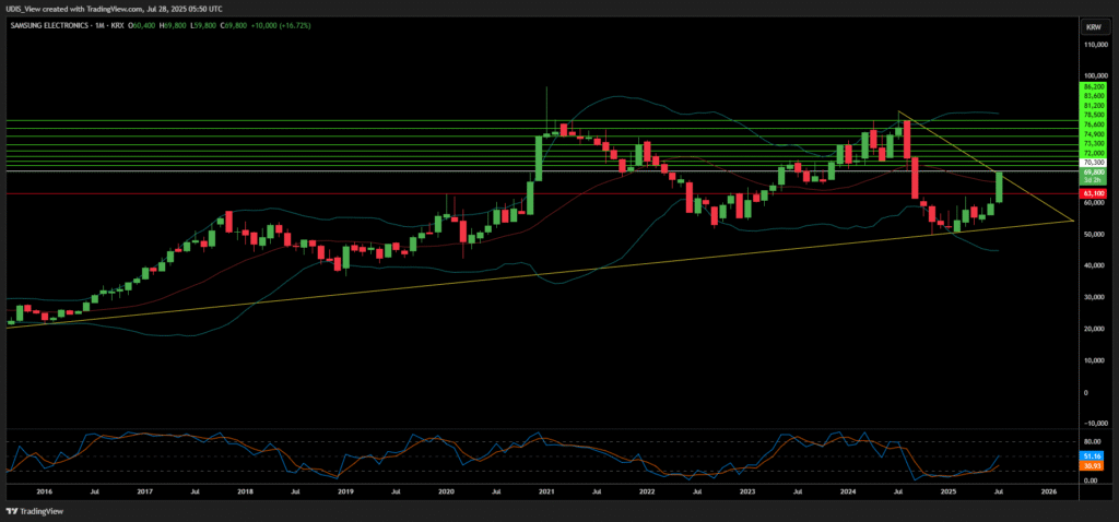
Samsung Long (Buy)
Enter At: 70,300
T.P_1: 72,000
T.P_2: 73,300
T.P_3: 74,900
T.P_4: 76,600
T.P_5: 78,500
T.P_6: 81,200
T.P_7: 83,600
T.P_8: 86,200
S.L: 63,100